Welcome to Worldia, we have over 25 years of expertise.

Top 10 CVD Diamond Types and How Are They Made?

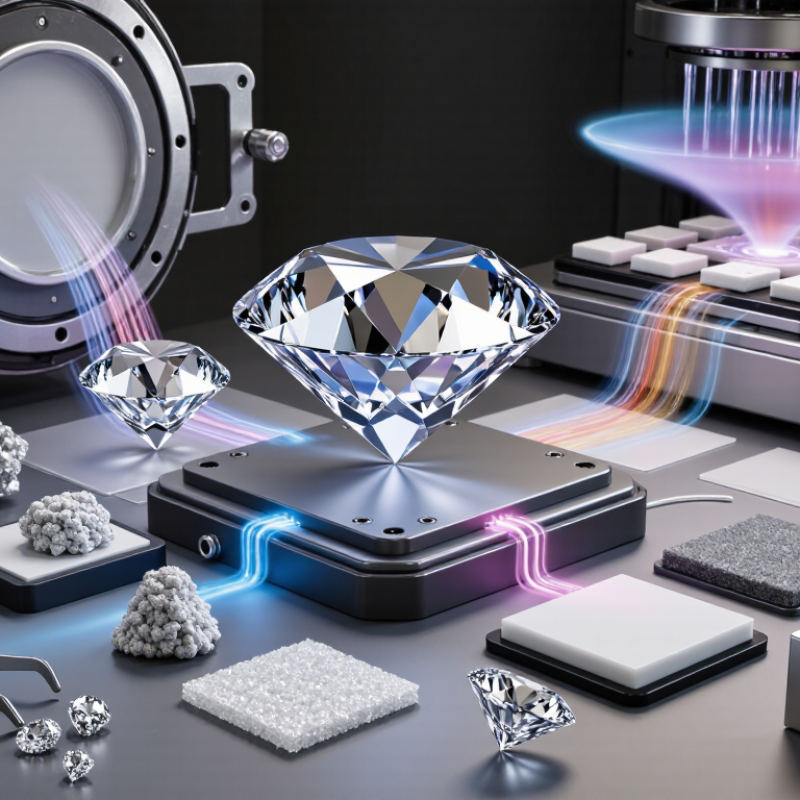
Diamond is more than a brilliant gemstone. It is an engineered material used in cutting tools, heat spreaders, optics, sensors, and research equipment. This guide examines ten important CVD diamond types and explains how their structures influence performance.

The Cvd Diamond Process grows diamond inside a controlled, low-pressure chamber. A carbon-containing gas, commonly methane, mixes with hydrogen above a heated substrate. Microwave plasma or a hot filament breaks the gases into reactive species. Carbon atoms then settle layer by layer, forming a diamond coating or crystal. Growth conditions matter greatly. Temperature, pressure, gas ratios, substrate preparation, and deposition time can change hardness, transparency, grain size, and thermal conductivity.

The ten types in this overview may be grouped by crystal form, grain structure, thickness, or controlled impurities. Examples include single-crystal, polycrystalline, microcrystalline, nanocrystalline, ultrananocrystalline, and doped CVD diamond. Some categories overlap. That is worth admitting. Industry terminology is not always perfectly consistent.

Real production also involves polishing, stress control, defect inspection, and careful quality testing. A glossy surface does not prove superior internal quality. Microscopy, Raman analysis, optical measurements, and thermal testing provide stronger evidence. Technical suppliers and laboratories may report different values because testing methods vary. Therefore, this article separates common manufacturing principles from performance claims that require verification. It aims to give readers a practical foundation, while recognizing that CVD diamond remains a demanding material to produce reliably. Small process changes can create large differences.
Top 10 CVD Diamond Types and How Are They Made?

What CVD Diamonds Are and How Their Growth Process Works

Top 10 CVD Diamond Types and How Are They Made?

CVD diamonds are grown, not mined. A thin diamond seed enters a sealed chamber with hydrogen and methane gases. Microwave energy creates a glowing plasma above the seed. Carbon atoms then settle onto its surface, layer by layer. Growth temperatures commonly reach 700–1,200°C, while chamber pressure stays far below atmospheric pressure.

The process sounds simple. It is not.

GIA technical literature explains that growth rate, gas chemistry, and temperature can create metallic inclusions, strain, or brown coloration. After growth, manufacturers may use heat treatment to improve color. Common CVD categories include single-crystal, polycrystalline, colorless, near-colorless, brown, pink, blue, treated-color, coated, and industrial-grade material. These labels describe structure, appearance, or use, rather than ten completely separate recipes.

Bain & Company’s 2023 Global Diamond Industry Report estimated laboratory-grown diamonds represented about 10% of diamond jewelry unit sales. That commercial rise makes traceable testing more important. The 2025 USGS Mineral Commodity Summaries lists synthetic diamond as a manufactured industrial material, but does not provide a dependable global production total. That missing figure deserves caution. Marketing claims often sound more precise than the public evidence.

In a laboratory, technicians monitor gas flow, plasma brightness, and crystal temperature continuously. A tiny shift can leave visible growth layers or reduce clarity. My own view is less romantic: CVD growth is controlled engineering, but it is not perfectly predictable. Each polished stone still needs independent grading and disclosure.
CVD Diamond Types and Representative Growth Rates

Chemical vapor deposition (CVD) diamond is formed when carbon-containing gases, commonly methane diluted in hydrogen, are activated by heat or plasma. The representative growth-rate ranges below vary with reactor design, methane concentration, pressure, substrate temperature, and plasma power.

Values are approximate literature-based ranges in micrometres per hour (µm/h), shown as lower and upper representative rates rather than fixed specifications.

How CVD Diamond Types Are Classified by Quality and Purpose

Top 10 CVD Diamond Types and How Are They Made?

CVD diamond types are classified by crystal quality, structure, and intended purpose. Single-crystal diamond offers the highest optical and thermal performance when defects remain low. Polycrystalline diamond contains many grains, making it practical for larger surfaces and industrial components. Microcrystalline material uses visible grains, while nanocrystalline diamond uses extremely small grains for smooth coatings. Homoepitaxial diamond grows on a diamond substrate with matching crystal orientation. The boundary is not always clean.

Manufacturers create these materials inside a controlled vacuum chamber. A carbon-containing gas, usually mixed with hydrogen, enters the chamber. Microwave plasma or a hot filament breaks the gas into reactive carbon species. These species deposit onto a heated substrate, building diamond layer by layer. Temperature, pressure, gas ratio, and growth time strongly affect quality. Small process changes can increase inclusions, stress, or surface roughness.

Purpose creates another useful classification. Optical-grade diamond needs high transparency and low absorption. Thermal-grade diamond prioritizes heat spreading and stable conductivity. Electronic-grade material requires controlled impurities and consistent electrical behavior. Doped CVD diamond can support sensors or specialized electrodes. Cutting-grade and protective coatings value hardness, adhesion, and wear resistance over visual clarity. Quality is relative to application. A cloudy film may fail in optics but perform well as a durable coating. Even experienced engineers must verify defects, thickness, and thermal performance instead of trusting a simple grade label.

The Main Stages of CVD Diamond Production

CVD diamond production begins with careful substrate preparation. A polished diamond seed is cleaned, inspected, and placed inside a sealed reactor. Its surface condition matters because scratches or contamination can disturb crystal growth. The reactor is then evacuated before controlled gases enter the chamber.

A hydrogen-rich mixture usually contains a small amount of methane. Energy from plasma or heated filaments breaks these gases into reactive species. Carbon atoms gradually attach to the seed surface, building a diamond layer one atom at a time. Growth temperature, pressure, gas flow, and plasma stability require constant monitoring. A minor temperature drift can change surface texture or create unwanted defects.

Growth is rarely perfectly uniform. That is an important practical limitation. Technicians may adjust the process during production, although frequent changes can reduce consistency. After growth, the crystal is cooled slowly to reduce thermal stress. It is then separated from the substrate, cut, and polished for its intended use. Inspection can include microscopy, spectroscopy, and measurements of color, thickness, and internal defects. Different conditions may produce transparent, colored, single-crystal, or polycrystalline CVD diamond. The final type depends heavily on gas chemistry, reactor design, growth time, and controlled impurities. Some results still need reassessment, especially when subtle defects are difficult to identify.

Top 10 CVD Diamond Types and How Are They Made? - The Main Stages of CVD Diamond Production
No. CVD Diamond Type Defining Characteristics Typical Growth Configuration Main Production Stages Typical Properties and Uses
1 Homoepitaxial Single-Crystal Diamond Diamond grows on a diamond substrate with the same crystal structure and lattice orientation, producing a continuous single-crystal layer. Microwave plasma CVD or hot-filament CVD; polished diamond seed; hydrogen-rich gas with a small hydrocarbon addition. Clean and orient the seed; mount it on the substrate holder; evacuate and hydrogen-purge the chamber; ignite the plasma; stabilize pressure, temperature, and gas flow; grow layer by layer; cool under hydrogen; remove and polish. High optical and thermal quality; used for optics, heat spreaders, high-power electronics, and research substrates.
2 Heteroepitaxial Single-Crystal Diamond Single-crystal diamond is deposited on a non-diamond substrate. The substrate can influence orientation, stress, defect density, and nucleation. Plasma-assisted CVD on a selected non-diamond substrate, often with an intermediate nucleation or buffer layer. Prepare and texture the substrate; enhance diamond nucleation; deposit an initial interface layer; establish oriented growth; continue thick-film deposition; remove the substrate when required; finish the diamond surface. Enables larger-area or specialized substrates; generally requires careful control of lattice mismatch, thermal stress, and defects.
3 CVD Polycrystalline Diamond Consists of many diamond grains with different orientations, separated by grain boundaries. Microwave plasma or hot-filament CVD on silicon, molybdenum, tungsten, carbide, or other suitable substrates. Roughen or seed the substrate; form a high-density nucleation layer; deposit diamond across the surface; allow grains to coalesce; increase thickness; cool, detach, or retain the substrate; grind and polish. Strong wear resistance and good thermal conductivity; widely used for cutting tools, wear parts, heat spreaders, and protective coatings.
4 Microcrystalline Diamond (MCD) Polycrystalline diamond with grains generally in the micrometre scale, commonly producing a relatively rough surface during growth. Hydrogen-rich CVD with comparatively moderate methane concentration and conditions that favor larger crystal grains. Prepare and seed the substrate; nucleate diamond; establish stable plasma chemistry; grow and enlarge crystallites; coalesce the film; remove or finish the surface by lapping or polishing. Low friction after suitable finishing and high abrasion resistance; used in machining tools, wear coatings, and mechanical components.
5 Nanocrystalline Diamond (NCD) Polycrystalline diamond with grains typically in the nanometre range, providing a finer and smoother microstructure than conventional microcrystalline films. Plasma CVD with higher nucleation density and gas chemistry adjusted to suppress excessive grain growth. Clean and intensively seed the substrate; generate dense nucleation; deposit a fine-grained layer; control grain growth and hydrogen chemistry; build the required thickness; polish or apply a finishing treatment. Smooth surface, high hardness, chemical resistance, and low wear; used in microelectromechanical systems, biomedical surfaces, optical parts, and precision tools.
6 Ultrananocrystalline Diamond (UNCD) Contains extremely small diamond grains and a relatively high fraction of grain-boundary material, resulting in distinctive mechanical, electrical, and surface behavior. Plasma-assisted CVD using gas chemistry and nucleation conditions designed for rapid formation of ultrafine grains. Prepare a highly nucleated surface; initiate ultrafine diamond growth; stabilize plasma power and carbon-to-hydrogen ratio; deposit the film; tailor grain-boundary chemistry if needed; finish and characterize. Very smooth, hard, wear-resistant, and chemically stable; used in microdevices, coatings, sensors, and tribological applications.
7 Boron-Doped CVD Diamond Contains boron incorporated into the diamond lattice, creating acceptor states and allowing semiconducting or electrically conductive behavior. CVD reactor supplied with a controlled boron precursor in addition to hydrogen and a carbon-containing gas. Prepare the substrate; establish diamond nucleation; introduce a calibrated boron precursor during growth; control dopant concentration and compensation; grow the layer; cool and anneal when required; pattern or contact the film. Electrical conductivity can be adjusted by dopant level; used for electrochemical electrodes, radiation detectors, sensors, and specialized electronic devices.
8 Nitrogen-Doped CVD Diamond Contains nitrogen-related defects or nitrogen incorporated during deposition; nitrogen can also affect growth rate, color, defect density, and optical absorption. CVD with a controlled nitrogen-containing gas addition, commonly in small concentrations relative to the hydrogen and hydrocarbon gases. Prepare and seed the substrate; ignite and stabilize the plasma; add nitrogen at a controlled flow; grow the diamond while monitoring defects and color; cool under controlled gas conditions; anneal or irradiate if a particular defect structure is required. Useful for studying nitrogen-vacancy-related optical and magnetic properties, as well as for tuning growth and material characteristics.
9 Isotopically Enriched CVD Diamond Diamond grown from a carbon source enriched in a selected isotope, most commonly a higher proportion of carbon-12 than in natural-abundance carbon. High-purity CVD reactor using isotopically controlled carbon-containing feed gas; other growth conditions are selected to minimize unwanted impurities. Clean the substrate and reactor; condition the chamber to reduce memory effects; introduce the isotope-controlled carbon feed; grow under stable plasma conditions; cool without contamination; characterize isotope composition and defects; polish or process the material. Reduced nuclear-spin noise can improve certain quantum and precision-sensing experiments; thermal and optical performance depends on purity and defect control.
10 Multilayer or Graded CVD Diamond Contains two or more CVD-grown layers with intentionally varied impurity concentration, grain structure, isotope content, stress, or electrical properties. Programmable plasma CVD with controlled changes in gas composition, pressure, temperature, plasma power, or substrate position during one or more growth runs. Prepare the substrate; grow the first layer; change the selected process parameter at a defined interface; deposit subsequent layers; repeat the transition for the required profile; cool under controlled conditions; polish and inspect interfaces. Allows properties to be tailored through thickness; used in electronic structures, optical components, sensors, thermal management, and engineered coatings.
Production note: Most CVD diamond processes share the same basic sequence: substrate preparation, surface cleaning and seeding, plasma or hot-filament activation, carbon-containing gas dissociation, diamond nucleation, controlled crystal growth, cooling, substrate removal when required, and final polishing or post-treatment. The categories above can overlap; for example, a film may be both nanocrystalline and boron-doped.

Ten CVD Diamond Types and Their Distinctive Features

Top 10 CVD Diamond Types and How Are They Made?

Ten CVD diamond types differ by crystal structure, grain size, chemistry, and surface condition. Single-crystal diamond grows on a diamond substrate inside a controlled plasma. It offers excellent thermal and optical performance. Polycrystalline diamond forms many grains on non-diamond substrates. It costs less, but grain boundaries can reduce heat flow. Microcrystalline diamond contains relatively large grains and provides strong wear resistance. Nanocrystalline diamond uses smaller grains for smoother coatings. Ultrananocrystalline diamond has extremely fine grains and a dense, hard surface.

Homoepitaxial diamond extends the lattice of a diamond seed with minimal crystal disruption. Heteroepitaxial diamond grows on another material, often producing more defects. Boron-doped diamond is made by adding a boron source during deposition. It can become electrically conductive and chemically stable.

Nitrogen-doped diamond uses controlled nitrogen additions, changing its color and defect structure. Silicon-vacancy diamond develops optical defects through silicon-containing gases or silicon-bearing substrates.

Hydrogen-terminated diamond receives a hydrogen-rich surface after growth. This treatment can improve surface conductivity. Isotopically enriched diamond uses methane with a selected carbon isotope, reducing lattice vibration and improving thermal behavior. Technicians commonly use microwave plasma or hot-filament systems, adjusting pressure, temperature, gas ratios, and substrate quality. The details matter. A small temperature shift can change grain size noticeably. These categories also overlap, so one sample may be nanocrystalline and boron-doped. The labels are useful, but never perfectly clean. Testing remains essential.

How Applications Influence CVD Diamond Selection

Top 10 CVD Diamond Types and How Are They Made?

How Applications Influence CVD Diamond Selection

CVD diamond is not one uniform material. Its performance depends on crystal structure, purity, thickness, doping, and surface finish. Microwave plasma CVD grows diamond from carbon-rich gas above a heated substrate. Hot-filament CVD uses a heated filament to activate the gas. Both methods require careful control of temperature, pressure, and gas composition.

Cutting tools usually need thick polycrystalline diamond with strong wear resistance. Its random grain structure handles varied cutting directions, but it may show more surface roughness. Heat spreaders often require high-purity single-crystal diamond. Low impurity levels support excellent thermal conductivity and reduce unwanted heat barriers. Optical windows demand controlled thickness, low absorption, and a carefully polished surface. Small defects can distort measurements. The application decides the priority.

Electrical uses may need boron-doped diamond, while electrochemical sensors require stable conductivity and chemical resistance. Medical and laboratory components often favor smooth, low-contamination surfaces. Size also matters. A large wafer can reduce assembly steps, yet growth may take longer and increase defect risks. A thinner film may be cheaper, but it can warp under heat or pressure. The match matters. A polished specification sheet can still mislead without testing the final component. In practice, I would compare thermal data, defect mapping, roughness, and coating adhesion under realistic operating conditions. No selection is perfect. Even experienced engineers sometimes value a headline property and overlook the manufacturing tolerance behind it.

Hi! What is your idea today?
WORLDIA 8618618272087
Nina +86 15631662072
google-site-verification=0STkOZEvYuoDp-D40AVfMUk--CzM2AsZv24S6ISPdmk